|
3 |
|
|
Implementation Method |
3.1 Data Path Changes
The original PDP-8 processor was produced to meet a target of costing under $20,000. This meant that the designers had restrictions imposed on them, which this project will not have.
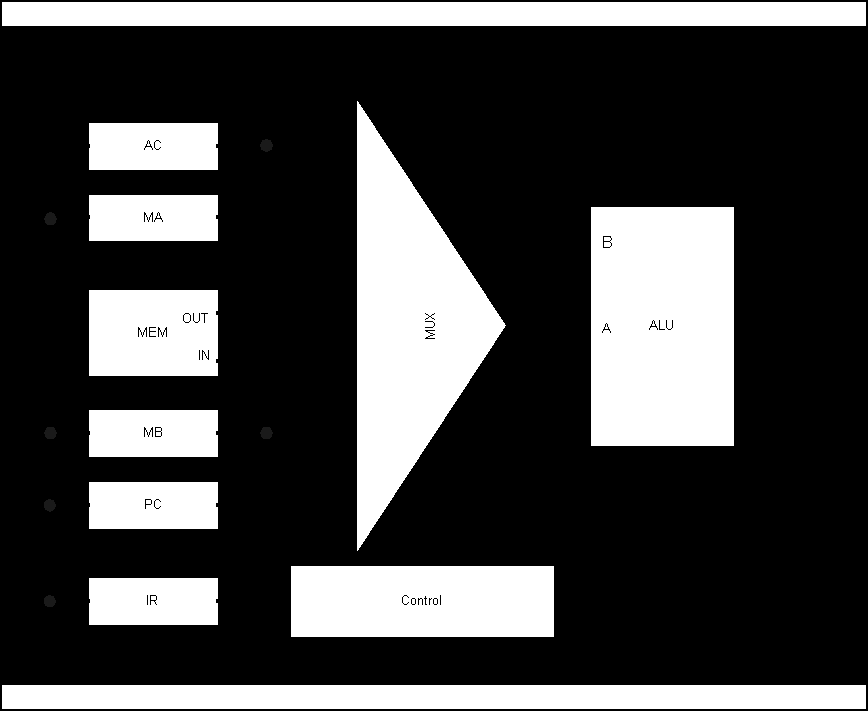
Below is the original data path diagram:

Fig 3.1 Original PDP-8 Data path Source: The Art of Digital Design, D Winkel & F. Prosser (Modified)
The data path for the new PDP-8 will be developed during the course of this chapter. It is important to introduce the old data path at this point in order to show the changes that will be made. We can see that there is a large multiplexer through which all the data passes. The registers are connected together along a single bus, which always passes through the ALU.
3.2 State Model
A state model is all possible states a processor can be in, it also defines movement between each state. The state model used for the PDP-8 required in the region of 20 states. It is unclear from the documentation if there are 17 real states with 3 additional states added for clarity but optimised away in the implementation or 20 real states. The aim of the new design is to reduce states drastically to less than 7.
The simplest optimisation here is to remove those states that cause the processor to wait for memory. This is possible due to the increased speed of the memory now available. Memory cycles in the original PDP-8 would send addresses to memory, then stall the processor until the memory returned a value.
3.3 Data Path Complexity
One reason for the state model to be so complex in the original machine is the number of buses available. Technology available at the time meant wires connecting blocks were expensive. For this reason the PDP-8 is built around a Uni-Bus design, each block is connected to the others via the ALU. This is shown in Fig 3.1. To reduce the number of states, data paths need to be added. This introduces the need for multiplexers, which will in tern reduce the operating speed. However, the intended performance gain from extra data paths should far outway the disadvantages of the multiplexers.
3.4 Choice of Implementation
There are a number of available methods to design the processor so that it could be targeted at a XILINX FPGA:
A schematic drawn implementation would have been far too time consuming for a processor the size of the PDP-8, especially because of its CISC nature, where the control is very irregular. The time spent laying out gates makes it unsuitable.
VHDL is a hardware description language, which can be simulated and compiled into gates.
A full VHDL implementation is feasible. The design could be made up from separate code modules and then combined in one top-level module. This design would have been very difficult to debug since the simulator would show only signal logic levels. There would be no easy way to understand top level schematic available in the simulator.
Verilog is another hardware description language. A full Verilog implementation has the same drawbacks as the VHDL design.
A combination of a hardware description language such as VHDL and hand drawn schematics is an ideal solution. The basis of the top-level design was drawn using a schematic editor and each module (e.g. the ALU) coded in VHDL. This was much easier to debug since it was possible to see data flowing between each of the components of the processor as well as to memory. Using a combination of VHDL and schematics also means that the processor can be retargeted at a different technology. All that is required is that the VHDL is recompiled for the new technology and the top level is technology independent. Having each block as a separate section of VHDL code allows for rapid prototyping and debugging.
The tools available on university machines give an ideal route from the combined description down onto a Xilinx array. Much of the process has been completed before, using similar software. The software used to design most of the project is Powerview.
3.5 Registers
The next important stage of the design is to determine what registers will be required. There must be enough registers to hold all the information required in every state, but not so many that some are used infrequently.
There are some registers which must automatically be included, e.g. Program Counter (PC), Accumulator (AC) and Instruction Register (IR).
|
Register |
Size (Bits) |
|
AC |
12 |
|
PC |
12 |
|
IR |
12 |
|
Link |
1 |
|
CA |
12 |
|
MB |
12 |
|
MA |
12 |
Fig 3.2 Initial Register List
Additional registers are required for a number of reasons. The Link register a 1 bit register is required to make the 13th bit of the accumulator used during rotate instructions. The CA (Contents of Address) register is used for storing data and addresses fetched from memory. MB (Memory Buffer) and MA (Memory Address) are used to preserve data and addresses respectively until it can be written to memory. We will see how these are used later.
3.6 Removed Items
There were some sections of the design that were not suitable to be implemented in a revised version of the PDP-8. The most notable of these is the switch register. This register is only modelled as, a register, but is actually a series of switches on the front of the computer. These can be OR’d with the Accumulator using the micro coded instruction
OSR. This instruction will not be implemented as per the original, it will instead be implemented as a "No Operation".Another component of the design to consider is manual operation. This feature allowed the user to step instruction by instruction through a program. The software supplied with the Xilinx FPGA allows for steps of one clock cycle to be executed. It was decided that this is much more suitable, due to the increased speed that the design will be able to achieve.
A manual step, operated by a physical switch, would have required the control to be more complex. The time required to implement a manual step was spent on more important sections of the design. The software control would give enough, had anything gone wrong on the board. The testing program also gives the advantage, that the assembler programs will have been tested in software. There should be no requirement to debug programs on the FPGA.
3.7 State Model Refinement
The state model needs to be substantially revised in order to meet the performance target of the project. The following actions are required:
This leads to the following state diagram:
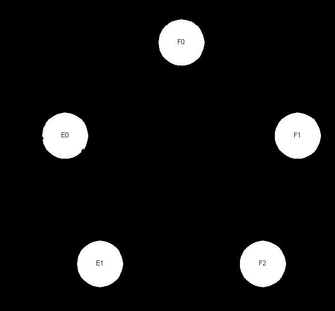
Fig 3.3 Initial State Diagram
This state diagram allows all instructions to complete and is much more efficient than the original state model. However there is still room for considerable improvement. The micro coded instructions are executed serially in the state E0, the aim is to integrate part of them into all the states. This will mean the only looping state is the idle state F0. The only micro coded instruction that would require looping would be a 2 bit rotate, which was originally implemented as two 1 bit rotates. It is sensible enough to have the shifter perform a 2 bit rotation, thanks to the larger transistor budget.
Auto Indexing requires an additional cycle to memory to write back the incremented memory location. However it is possible to increment the value and write it to memory later. This removes the need for the state E1. The auto index instructions can follow the path between F2 and E0.
3.8 Initial Data Path
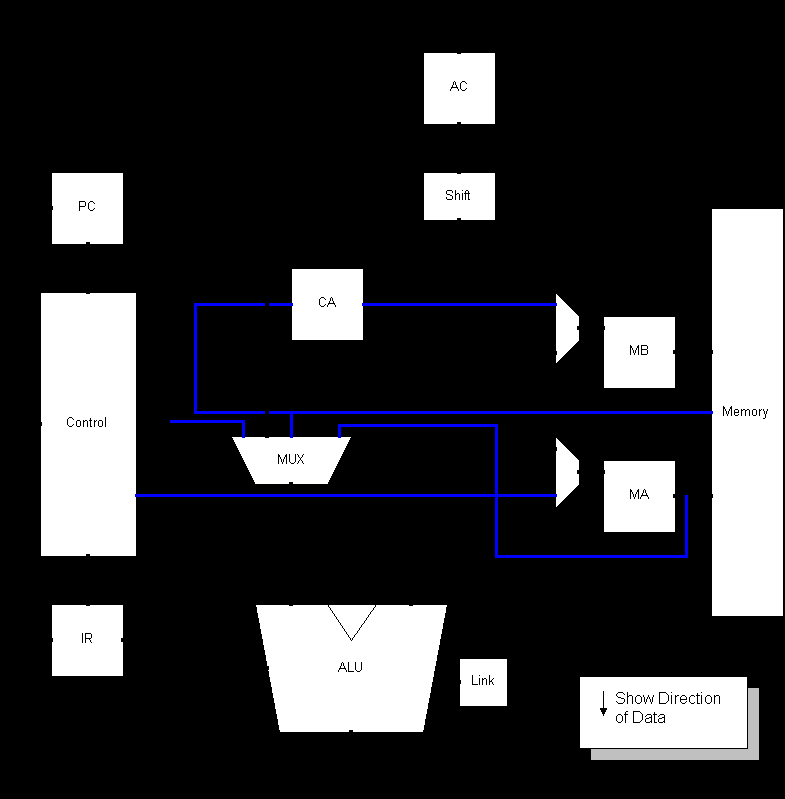
Fig 3.4 Initial Data Path Design
This initial data path is very closely linked to the original data path of the PDP-8. One of the most noticeable differences is that the Accumulator is only connected to one port of the ALU. This reduces the size of the mulitplexer feeding the ALU port A but increases the complexity of the ALU. The ALU must now be able to pass values through unchanged on either port. When considered this isn’t difficult, simply add the chosen port to zero.
The micro coded instruction set contains the shift operations, which can also be used in conjunction with the increment accumulator. The specification requires that the increment be completed before the shift. In the initial data path two cycles would be required to complete both operations. By swapping the order of the shifter and AC as shown in Fig 3.5 it is possible to complete this operation in a single cycle.
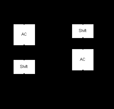
Fig 3.5 Shifter Rearrangement
This simple rearrangement will give an increase in speed of the frequently used increment and rotate instructions.
Whilst looking at the shift it also became obvious that the Link register should also be located next to the accumulator, rather than being connected to the ALU.
The data paths were tested manually at each stage to ensure that a bus was never used by two blocks at the same time or unused. The testing uncovered a number of problems with holding memory addresses and data until such time that the memory was free. There were also cases where the memory buffer wasn’t required at all. The memory interface was redesigned as shown in Fig 3.5.
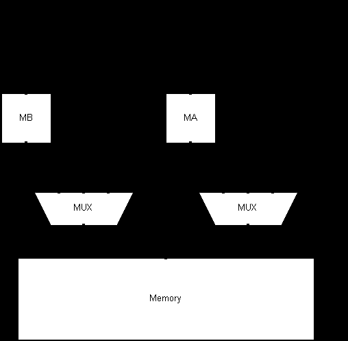
Fig 3.6 Memory Interface
The revised memory interface allows data to be stored for a cycle into the MA or MB registers or bypassed and written straight to memory. There is also a third port, which has been added to the multiplexer. This is a connected to the buses from other parts of the processor as labelled. The content of AC is usually what is being stored to memory and EA is usually the address to fetch from memory. It is therefore suitable to give them a direct route to memory. This arrangement also makes the auto index write back possible while the rest of the processor is working on performing a TAD instruction. In practice the memory interface is much more complex and requires control to determine if a read or write operation is being made, also if the memory is enabled. The board onto which the PDP-8 is being targeted has already been used for the design of a 16-bit processor with a memory interface. The PDP-8 re-implementation will use the bottom 12 bits of the existing 16-bit memory interface.
3.9 Program Counter
The program counter in the PDP-8 does not start from 0. Instead it needs to start from 2008. This allows execution to start at the beginning of page 1 in memory. In order to get an initial value of 2008 which is 0000100000002 only one bit must be set. This is achieved by inverting the input and output of register for bit 7. Fig 3.7 shows how this is achieved.
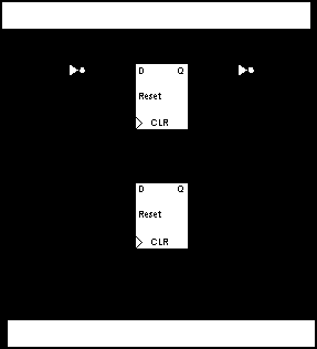
Fig 3.7 Modifications to PC for initial value
The program counter, bit 7, will always store the inverse of the current bit, but since both input and output are inverted the correct value is passed out of the PC. On initial reset all bits will be zero, but the output of bit 7 will be inverted giving ‘1’, hence a program counter of 2008.
3.10 Output Requirements
Some blocks, e.g. the AC, need to generate test signals such as equal to zero. These are used in either micro coded or normal skip instructions. The following outputs are required
|
Block |
Output |
Mnemonic |
|
ALU |
Result Zero |
ALU_ZERO |
|
AC |
Negative AC |
NEG_AC |
|
Zero AC |
ZERO_AC |
|
|
LINK |
Zero Link |
ZERO_L |
Fig 3.8 Block Outputs
3.11 Final State Diagram
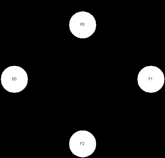
Fig 3.9 Final State Diagram
The revised state model shown in Fig 3.9 removes the redundant states and looping of micro coded execution. All microcoded instructions are executed by following the indirect execution path. In each state part of the microcoded instruction is executed. This optimisation reduces the execution time and simplifies the processor control.
Auto indexing is now carried out during the indirect state, but the incremented address is written back to memory later.
3.12 Variable Instruction Time
The CISC nature of the processor means that instructions take different times to complete. For example a Twos Complement Addition (TAD) takes 3 cycles using direct addressing, but 4 cycles when using indirect addressing. The following table shows a complete list of the instruction time:
|
Instruction |
Addressing Mode |
State F0 |
State F1 |
State F2 |
State E0 |
|
DCA |
Direct |
ü |
ü |
||
|
Indirect |
ü |
ü |
ü |
||
|
TAD |
Direct |
ü |
ü |
ü |
|
|
Indirect |
ü |
ü |
ü |
ü |
|
|
Auto Index |
ü |
ü |
ü |
ü |
|
|
JMP |
Direct |
ü |
ü |
||
|
Indirect |
ü |
ü |
ü |
||
|
ISZ |
Direct |
ü |
ü |
ü |
Cond. |
|
Indirect |
ü |
ü |
ü |
ü |
|
|
JMS |
Direct |
ü |
ü |
ü |
|
|
Indirect |
ü |
ü |
ü |
Fig 3.10 Instruction Execution Length
There is still a problem with this state diagram. The Indirect Skip instruction requires 5 states to complete. At first it looks as though the extra Execution State must be reintroduced, however, the final cycle of the instruction is conditional and may not be executed. This instruction is used very infrequently, so to keep the entire system performance up and to keep the state space small this instruction will incur a 2-cycle penalty. This is to say that if the ALU result is zero and the conditional state must be executed and next instruction should be skipped. The next instruction is skipped by incrementing the PC again. To get around this the next instruction will be fetched but not executed. The consequence of this means the programmer will be unaware of the underlying changes.
3.13 Microcoded Instruction Mapping
The micro-coded instructions have been mapped onto states so that the priority ordering is adhered to. All micro-coded instructions will now complete in the 4 states and in the same time as any normal indirect instruction, no matter how many operations need to be performed as part of the instruction. Fig 3.11 shows the mapping
|
Micro code Group |
State |
Instruction |
|
1 |
F1 |
CLA, CLL |
|
1 |
F2 |
CMA, CML |
|
1 |
E0 |
Inc and Rotates |
|
2 |
F1 |
Skips |
|
2 |
F2 |
CLA, Halt |
Fig 3.11: Micro-coded State Mapping
3.14 Final Data Path
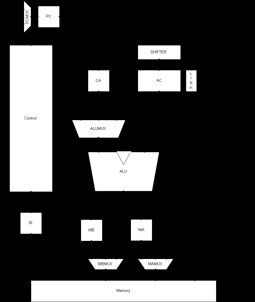
Fig 3.12 Final Implementibe Data Path
Fig 3.12 shows the diagram that was used to design the top level of the processor. It is complete in every detail, other than the control signals. Control signals where no shown as it would have complicated the diagram.
3.15 Signal to State Assignment
The next section of the design was to determine which signals need to change in which states and which need to remain unchanged. The process is very time consuming and requires manual processing of instructions through the final data path design. Fig 3.14 shows an example of the standard fetch (F0) State. The lighter coloured busses are those that have data flowing on them in this state and the IR register is being loaded.
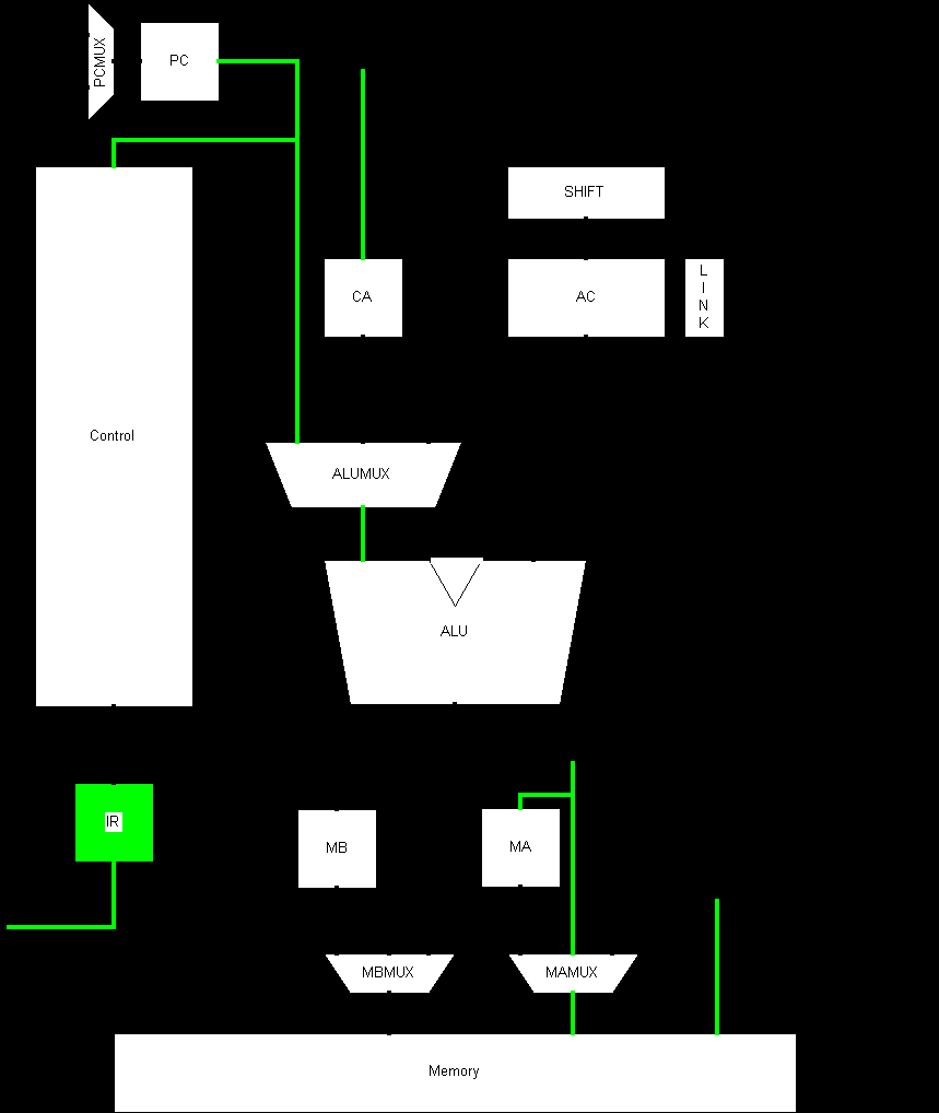
Fig 3.13 Signal to State assignment
See Appendix A for a full signal assignment table.
This type of analysis of bus and register usage proved effective in finding deficiencies at all stages of the data path development.
3.16 VHDL Coding
The majority of the project time was allocated to writing and debugging the VHDL code that describes each of the logic blocks shown in the data path. The need to draw the top level of the design as a schematic, was shown earlier, have each block as its own VHDL code. The project environment was set up in Powerview and a schematic started for the top level.
The best place to start is to design the simplest component in VHDL in order to test that the environment has been set-up correctly. The code below is for the program counter multiplexer.
library IEEE;
use IEEE.std_logic_1164.all;
entity MUX_12BIT2x is
port (
D1: in STD_LOGIC_VECTOR (11 downto 0);
D2: in STD_LOGIC_VECTOR (11 downto 0);
SEL: in STD_LOGIC;
Q: out STD_LOGIC_VECTOR (11 downto 0)
);
end MUX_12BIT2x;
architecture MUX_ARCH2x of MUX_12BIT2x is
BEGIN
PROCESS (SEL,D1,D2)
BEGIN
CASE SEL IS
WHEN '0' => Q <= D1;
WHEN '1' => Q <= D2;
WHEN OTHERS =>
-- shouldn't occur, since bit patterns in correct
END CASE;
END PROCESS;
END MUX_ARCH2x;
This code illustrates the use of standard VHDL types. The line
D1: in STD_LOGIC_VECTOR (11 downto 0); defines that the input D1 will be an 12 bit input and that Q the output of the multiplexer is also 12 bits. There are two main sections to the code, ‘entity’ and ‘architecture’. The entity describes the interface to the block and the architecture is the details of its internal workings, in this case a multiplexer. It should be possible to understand the code for a multiplexer without any knowledge VHDL.The VHDL code for blocks is entered into files with a .vhdl extension. These are then loaded in the Powerview VHDL Manager. The manager checks and compiles the VHDL into a testable form. This process must be performed on each module before it can be used in a schematic design.
Since the top-level schematic is hand drawn, the symbols for each of the block have already been designed. These are assigned to be composite blocks and have attributes, which point the correct VHDL file to describe their behaviour.
The top-level data path was the first major mile stone in the processor design, complete on 29 Nov 1999. All the logic blocks had been placed into the schematic and all hand drawn busses added. See Appendix B2 for a full top level schematic.
The next stage was to complete some more logic blocks in order to test basic functionality of a few blocks when working the top-level schematic. All registers in the processor are based on standard VHDL modelled D-Type flip-flops. Some blocks, e.g. AC, need to have extra logic around them in order to generate test values, such as AC equal to zero and negative AC.
The ALU is the second largest block in the processor. It only needs to perform a limited number of functions; Addition, And, Increment and Or. However, increment needs to be able to increment both ports of the ALU. All increments are specified as two’s compliment, but the PC must be an unsigned increment. The design of an ALU is fairly simple and well documented making it much easier.
The control logic holds the key to the design. It is this section of VHDL that will control the entire processor. It will contain registers, which will hold state about the processor, mainly the current execution state. The memory address for direct data fetching is calculated by the control.
The control block is written in VHDL ins such way that each state is a function. This allows the body of the control to look like a call back function. The main control loop keeps looping, calling the correct function. Following a function call a function,
nextstate, is called which returns the state to move to next. The control models the execution steps shown in Fig 3.9.There are a number of processes in the control; those responsible for latching data into registers are synchronised with the clock. This ensures that the data will flow to the registers and will be stable by the time the register is latched.
3.17 VHDL to Gates
In order for a VHDL design to be run on a hardware device it must first be converted to gates or configurable logic blocks (CLB). The Poweview software available will not handle CLB simulation, so the design must be converted to gates. In order for this conversion to take place, the VHDL descriptions need to be exported to an application called Synopsys. This is will optimise and compile the design.
At this point in design problems started to occur. Firstly the Synopsys software was not set up to target the Xilinx device being used and the VHDL code already written was not functionally identical when converted to gates. Following many days of re-writing VHDL some of the blocks were converted to gates. Having compiled the design to gates the lengthy process of exporting from Synopsys in another file format (EDIF) began. This caused a few problems due to Powerview requiring different labelling on busses where compared to Synopsys. These problems were resolved and logic blocks were tested using their gate equivalents.
Testing uncovered a number of inconsistencies between the function of the VHDL and gate level equivalent designs. The discrepancy between the two was mainly do some VHDL incorrectly describing registers as flip-flops. The entire process took in the region of 3 weeks. Some further changes were required to the signals in the control to ensure timing constraints were met.
3.18 Xilinx Generation
Having tested a full gate implementation of the new PDP-8 it was possible to start the process of downloading the processor onto an FPGA. In order for a design to be loaded onto a Xilinx the design must be analysed and converted into Configurable Logic Blocks (CLBs). There are Xilinx tools available, which automate this process. Within an hour the processor was on the FPGA.